Semiconductor Materials and Semiconductor Devices – Semiconductors: NEET MCQs with Answers
15 free questions on Semiconductor Materials and Semiconductor Devices – Semiconductors for NEET (UG), starting with previous-year NEET and AIPMT questions. Try each one, then tap Show answer for the answer and a short explanation.
Syllabus covered: Semiconductors; semiconductor diode: I-V characteristics in forward and reverse bias; diode as a rectifier; I-V characteristics of LED. the photodiode, solar cell, and Zener diode; Zener diode as a voltage regulator.
Question 1
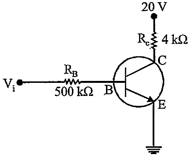
Previous-year questionIn the circuit shown in the figure, the input voltage Vᵢ is 20 V, V_BE = 0 and V_CE = 0. The values of I_B, I_C and β are given by [NEET 2018]
- I_B = 40 μA, I_C = 10 mA, β = 250
- I_B = 25 μA, I_C = 5 mA, β = 200
- I_B = 40 μA, I_C = 5 mA, β = 125
- I_B = 20 μA, I_C = 5 mA, β = 250
Show answer
Answer: (C) I_B = 40 μA, I_C = 5 mA, β = 125
Explanation: With V_BE = 0, I_B = 20/500 kΩ = 40 μA. With V_CE = 0, I_C = 20/4 kΩ = 5 mA. Hence β = I_C/I_B = 5 × 10⁻³/40 × 10⁻⁶ = 125.
Question 2
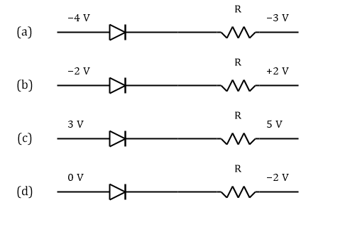
Previous-year questionWhich one of the following represents a forward biased diode? [NEET 2017]
- Option (a)
- Option (b)
- Option (c)
- Option (d)
Show answer
Answer: (D) Option (d)
Explanation: Forward bias requires the p-side (the left terminal in each diagram) to be at a higher potential than the n-side. With 0 V at the p-side and –2 V beyond the resistor, the p-side is 2 V higher, so this diode is forward biased. In the –4 V / –3 V, –2 V / +2 V and 3 V / 5 V connections the p-side is at the lower potential, so those diodes are reverse biased.
Question 3
Previous-year questionThe increase in the width of the depletion region in a p-n junction diode is due to [NEET 2020]
- Reverse bias only
- Both forward bias and reverse bias
- Increase in forward current
- Forward bias only
Show answer
Answer: (A) Reverse bias only
Explanation: Reverse bias adds to the built-in potential and pulls majority carriers further away from the junction, widening the depletion layer. Forward bias does the opposite, narrowing it.
Question 4
Previous-year questionFor a p-type semiconductor, which of the following statements is true? [NEET 2019]
- Electrons are the majority carriers and trivalent atoms are the dopants
- Holes are the majority carriers and trivalent atoms are the dopants
- Holes are the majority carriers and pentavalent atoms are the dopants
- Electrons are the majority carriers and pentavalent atoms are the dopants
Show answer
Answer: (B) Holes are the majority carriers and trivalent atoms are the dopants
Explanation: A p-type crystal is made by doping with trivalent (acceptor) atoms such as boron, indium or aluminium. Each acceptor creates a vacancy in a covalent bond, so holes become the majority carriers and electrons the minority carriers.
Question 5
Previous-year questionIn a p-n junction diode, a change in temperature due to heating [NEET 2018]
- Affects only the reverse resistance
- Affects only the forward resistance
- Affects the overall V–I characteristics of the p-n junction
- Does not affect the resistance of the p-n junction
Show answer
Answer: (C) Affects the overall V–I characteristics of the p-n junction
Explanation: Raising the temperature increases the number of thermally generated carriers, which lowers the barrier potential, increases the forward current at a given bias and sharply increases the reverse saturation current. Both branches of the characteristic – indeed the whole curve – are affected.
Question 6
Previous-year questionThe input signal given to a CE amplifier having a voltage gain of 150 is Vᵢ = 2 cos(15t + π/3). The corresponding output signal will be [AIPMT 2015]
- 75 cos(15t + 2π/3)
- 2 cos(15t + 5π/6)
- 300 cos(15t + 4π/3)
- 300 cos(15t + π/3)
Show answer
Answer: (C) 300 cos(15t + 4π/3)
Explanation: The amplitude is multiplied by the gain: 2 × 150 = 300. A common emitter stage also introduces a phase reversal of π, so the phase becomes π/3 + π = 4π/3.
Question 7
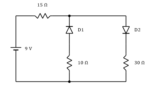
In the circuit shown, D1 and D2 are ideal diodes and the 9 V cell has negligible internal resistance. The current supplied by the cell is
- 0.2 A
- 0.36 A
- 0.3 A
- 0.4 A
Show answer
Answer: (A) 0.2 A
Explanation: The cell tends to send current downward through both branches. D2 is forward biased and acts as a plain wire, while D1 is reverse biased and acts as an open switch, so the 10 Ω branch carries no current. The circuit reduces to 15 Ω and 30 Ω in series, giving I = 9/45 = 0.2 A.
Doing well? Create a free account to take timed tests on this topic and see your weak areas.
Question 8
Silicon at 300 K, with intrinsic carrier concentration nᵢ = 1.5 × 10¹⁰ cm⁻³, is doped with a pentavalent impurity of concentration 2 × 10¹⁵ cm⁻³, all of it ionised. The electron mobility at this doping is 1000 cm² V⁻¹ s⁻¹. Find the electron concentration nₑ, the hole concentration n_h and the conductivity σ. (e = 1.6 × 10⁻¹⁹ C)
- nₑ = 2 × 10¹⁵ cm⁻³, n_h = 1.5 × 10¹⁰ cm⁻³, σ ≈ 0.32 S/cm
- nₑ = 2 × 10¹⁵ cm⁻³, n_h = 1.1 × 10⁵ cm⁻³, σ ≈ 3.2 S/cm
- nₑ = 1.1 × 10⁵ cm⁻³, n_h = 2 × 10¹⁵ cm⁻³, σ ≈ 0.32 S/cm
- nₑ = 2 × 10¹⁵ cm⁻³, n_h = 1.1 × 10⁵ cm⁻³, σ ≈ 0.32 S/cm
Show answer
Answer: (D) nₑ = 2 × 10¹⁵ cm⁻³, n_h = 1.1 × 10⁵ cm⁻³, σ ≈ 0.32 S/cm
Explanation: Pentavalent doping makes electrons the majority carriers, so nₑ = 2 × 10¹⁵ cm⁻³. The mass-action law gives n_h = nᵢ²/nₑ = (2.25 × 10²⁰)/(2 × 10¹⁵) ≈ 1.1 × 10⁵ cm⁻³. The holes are far too few to matter, so σ = nₑeμₑ = 2 × 10¹⁵ × 1.6 × 10⁻¹⁹ × 1000 = 0.32 S/cm.
Question 9
An n-type silicon sample of donor concentration N_D is at a temperature where all the donors are ionised, while thermal generation of electron-hole pairs is still far smaller than N_D. If nₑ and n_h are the electron and hole concentrations, which statement is definitely true?
- nₑ < n_h
- nₑ is about N_D and is far greater than n_h, with n_h not zero
- nₑ is about N_D, and n_h is exactly zero
- nₑ = n_h
Show answer
Answer: (B) nₑ is about N_D and is far greater than n_h, with n_h not zero
Explanation: With all donors ionised and few thermally generated pairs, the electron concentration is close to N_D. The holes satisfy nₑn_h = nᵢ², so n_h = nᵢ²/nₑ, which is very small compared with nₑ. It is not zero, because thermal generation always produces a few pairs.
Question 10
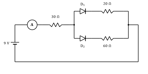
In the circuit shown, the battery of 9 V has negligible internal resistance, and D₁ and D₂ are ideal diodes. What is the reading of the ammeter?
- 0.18 A
- 0.20 A
- 0.10 A
- 0.30 A
Show answer
Answer: (B) 0.20 A
Explanation: The positive terminal of the battery drives current through both diodes in their forward direction, so each acts as a short circuit. The 20 Ω and 60 Ω branches are then in parallel, giving 20 × 60/80 = 15 Ω. The total resistance is 30 + 15 = 45 Ω, so the current is 9/45 = 0.20 A.
Question 11
A 36 V battery of negligible internal resistance, a 12 Ω resistor and a section AB are joined in series. Section AB has two parallel branches: a 12 Ω resistor alone, and an ideal forward-biased diode in series with another 12 Ω resistor. What is the potential difference across AB?
- 12 V
- 18 V
- 24 V
- 36 V
Show answer
Answer: (A) 12 V
Explanation: The forward-biased ideal diode has zero resistance, so section AB is 12 Ω in parallel with 12 Ω, which is 6 Ω. The total resistance is 12 + 6 = 18 Ω and the current is 36/18 = 2 A. The potential difference across AB is 2 × 6 = 12 V.
Question 12
In the circuit shown, the battery has an emf of 6 V and negligible internal resistance, and D₁, D₂ and D₃ are ideal diodes. What current does the battery supply?
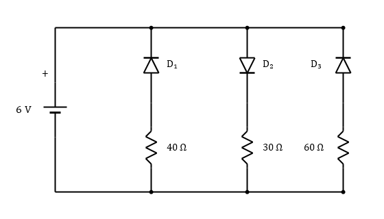
- 0.45 A
- 0.35 A
- 0.20 A
- 0.25 A
Show answer
Answer: (C) 0.20 A
Explanation: The top wire is at the higher potential. Only D₂ points from the top wire to the bottom wire, so it alone is forward-biased, while D₁ and D₃ are reverse-biased and act as open switches. Current flows only through the 30 Ω branch, so I = 6/30 = 0.20 A.
Question 13
The resistivity ρ of a pure semiconductor is measured while its temperature T is raised steadily. Which description fits the ρ–T curve?
- ρ rises nearly linearly with T
- ρ falls steeply at first and then more slowly, in a roughly exponential decay
- ρ rises slowly at first and then sharply
- ρ stays almost the same at all T
Show answer
Answer: (B) ρ falls steeply at first and then more slowly, in a roughly exponential decay
Explanation: Raising the temperature breaks more covalent bonds, so the number of electrons and holes grows very rapidly. This growth far outweighs the small fall in relaxation time. The resistivity therefore decreases, roughly exponentially, which is the opposite of the behaviour of a metal.
Question 14
A silicon crystal doped with a small amount of boron is cooled to 0 K. Which statement correctly describes the crystal at this temperature?
- It has equal numbers of free electrons and holes.
- It has no free electrons or holes available for conduction, so it behaves like an insulator.
- It has free electrons in the conduction band but no holes.
- It has free holes from the acceptor atoms but no free electrons.
Show answer
Answer: (B) It has no free electrons or holes available for conduction, so it behaves like an insulator.
Explanation: At 0 K there is no thermal energy to lift electrons out of the valence band. The conduction band stays empty, and electrons cannot rise even to the acceptor levels, so no holes are formed either. With no mobile carriers the doped crystal behaves like an insulator, and holes appear only when the temperature is above 0 K.
Question 15
How is the circuit symbol of a Zener diode told apart from that of an ordinary p-n junction diode?
- Two small arrows point away from the symbol
- Two small arrows point towards the symbol
- The triangle is drawn with no bar at its tip
- The bar at the tip of the triangle has bent ends, giving it a Z-like shape
Show answer
Answer: (D) The bar at the tip of the triangle has bent ends, giving it a Z-like shape
Explanation: A Zener diode is drawn like an ordinary diode, except that the bar at the tip of the triangle has its ends bent so that it suggests the letter Z. Arrows pointing towards a diode symbol mark a photodiode, and arrows pointing away mark an LED. An ordinary diode has a straight bar.
Want more Semiconductor Materials and Semiconductor Devices – Semiconductors questions?
E-GYAN NIDHI has 369 questions on this topic and 63,000+ in total, all free: timed CBT tests, NEET marking and instant analysis.
Register free Free Sunday Mock Test